


Under the US CHIPS Act, the National Semiconductor Technology Center (NSTC) is poised to emerge as a public-private consortium, comprising stakeholders from government, industry, academia, entrepreneurship, labour representatives, and investors, with the aim of advancing innovation from research laboratories to manufacturing facilities.
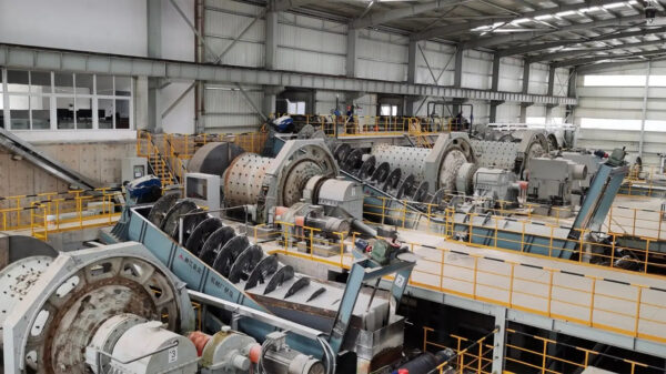
Experts highlight the importance of expanding domestic manufacturing capacity to lessen dependence on offshore production. Majority of semiconductor manufacturing takes place overseas, with an even higher reliance on foreign resources for packaging, advanced packaging, and heterogeneous integration.
Several industry groups, such as the American Semiconductor Innovation Coalition (ASIC) and MITER Engenuity, have put forward recommendations for the NSTC and proposed the establishment of the National Advanced Packaging Manufacturing Program (NAPMP).
There is a need for specialist firms joining forces to produce currently unachievable solutions. As the industry becomes increasingly driven by system requirements – the era of single companies providing comprehensive solutions has ended.
MITER Engenuity directs the Semiconductor Alliance, encompassing US semiconductor firms responsible for over half of the domestic industry’s research and development, as well as prestigious American universities.
NSTC collaborates with foreign organisations, such as Belgium-based Imec, to avert duplicating previous efforts. Imec’s CEO, Luc Van den hove, confirmed their eagerness to support the NSTC in any capacity required.
Collaborative networks could be constructed that include existing establishments such as the Institute at the Albany NanoTech Complex in New York and the Lincoln Laboratory at MIT. Albany Nanotech, which maintains the sole 300mm wafer facility built using US public funds, has formed alliances with major industry players such as IBM, GlobalFoundries, Samsung Electronics, Applied Materials, Tokyo Electron, ASML, and Lam Research.
Raj Jammy, an executive director of Semiconductor Alliance stressed the paramount importance of creating a robust network of research institutes and allies. He referenced examples like Silicon on Insulator (SOI) technology for power electronics and praised the Institute of Microelectronics (IME), an arm of the Singapore Agency for Science, Technology and Research, for its remarkable packaging capabilities.
The NSTC wants to rely less on China. But he competition with China is a long-term challenge. It’s important to keep semiconductor manufacturing safe and let the US and its allies lead the industry. They need to balance business goals and security.
Most of the world’s semiconductor packaging is outside the US, in places like China and Taiwan. This is a big problem for the US. Low-wage Asian countries have an advantage because packaging needs many workers. However, more automation could bring the industry back to the US.
Companies like TSMC and Intel are good at high-performance packaging, which is becoming more like semiconductor manufacturing. If the US can do this, it can grow the industry at home. TSMC and Intel are building new factories in the US thanks to the CHIPS Act.
The US plans to build 13 new semiconductor factories soon, but it needs to find enough engineers and technicians. In the next five years, the US will need 50,000 new engineers, which is twice the number of local graduates.
To fill this gap, the US might need to change visa rules to attract foreign talent – particularly from Asia. The government, schools, and businesses will work together to find more talent in the US, including hiring people with H1-B visas.