


Tokyo Electron (TEL), the fourth largest global semiconductor equipment manufacturer based in Japan, has been the centre of industry buzz with its recently developed hybrid oxide etch equipment. This new device is garnering exceptional interest from the device industry, particularly Samsung Electronics, due to its notably high-speed etching capability and the elevated level of precision achieved with the end results.
Industry sources on 18th May confirmed that TEL plans to install a demonstration version of the hybrid oxide etching device at a location earmarked by the Samsung Electronics Semiconductor Research Center. The novel aspect of TEL’s oxide etching equipment is that it incorporates a direct current (DC) pulse generator as an energy source, alongside the more traditional radio frequency (RF) generator.
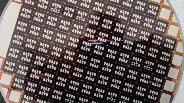
The plasma formation within the etching equipment chamber necessitates an injection of energy into the gas, leading to ionisation. It is with the ions and radicals generated at this juncture that fine pattern etching is executed. Historically, RF power was the sole energy source for ionisation, but with the evolution of the oxide etching process leaning towards narrower and deeper drilling of the insulating film, an increased power intensity becomes necessary.
This, however, leads to the challenge of frequent arcing – where sparks fly within the chamber during the process – as well as the expansion of equipment size when RF generator output increases. In response to these issues, US-based Lam Research, who holds over 60% of the etching equipment market share within Samsung Electronics’ semiconductor division, has focused on equipment development that mitigates arcing whilst amplifying RF power output.
TEL’s innovative approach involved the use of a DC pulse generator that applies a negative voltage while deploying suitable RF power. This groundbreaking method, an industry first, uses RF for deep drilling and DC pulses for precise shaping. The company has also ingeniously developed a structure that introduces metal into the etching gas, aligning with the hybrid etching equipment that uses RF and DC pulses as power sources.
Test wafers were sent by Samsung Electronics to TEL headquarters in Japan for evaluation, and the resulting report received positive feedback from field engineers due to the swift etching speed and smoothly shaped patterns. It is expected that TEL’s hybrid oxide etching equipment will be utilised in drilling the channel hole, a critical aspect of Samsung Electronics’ 3D NAND flash production process.
Industry experts forecast a significant shift in the share of oxide etching equipment within Samsung Electronics, contingent upon positive evaluation results after the TEL demo machine installation.
It is suggested that Lam Research is already preparing to respond to this development. Locally, APTC, a company associated with SK Hynix, is also reportedly developing similar oxide etching equipment as TEL. A number of related patents have been registered or are pending, and it is anticipated that tangible development results will emerge next year.
It is worth noting that the oxide etching market constitutes more than half of the total etching equipment market, according to industry sources. Therefore, successful development and customer adoption of a hybrid oxide etching machine could significantly boost sales for companies such as APTC.