


Recognising the strategic importance of semiconductor package technology, the South Korean government is set to pioneer extensive research and development (R&D) ventures in an attempt to bridge the gap with international market leaders, such as Taiwan’s TSMC. This new endeavour aims to not only harness advanced technologies in specialised areas but also take the helm as a primary innovator.
The R&D project, budgeted at an upper limit of 500 billion won ($390.6 million), necessitates the clearance of a preliminary feasibility study. According to authoritative sources within the Ministry of Trade, Industry and Energy, the Korea Evaluation Institute of Industrial Technology, and industry insiders, the ‘Semiconductor Advanced Packaging Leading Core Technology Development Project’ is currently in the works.
The government is reportedly ascertaining private sector interest and evaluating individual company capacities for this ambitious endeavour. With a timeline spanning five to seven years, the project is anticipated to cost between 300 billion and 500 billion won ($234-390.6 million). The planning process is being helmed by Park Yong-chul, the former CEO of Amkor Korea, who has assumed the position of chairman of the promotion committee.
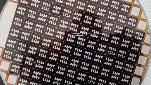
The advanced package R&D project can be broadly categorised into two types: catch-up and lead. The former aims to boost domestic capabilities in areas such as heterogeneous integration, wafer-level package (WLP), panel level package (PLP), and high-density flip chip, sectors currently dominated by Taiwan’s TSMC, America’s Amkor, and China’s JCET group.
“With the aim of breaking into the package market monopolised by a handful of companies and dramatically narrowing the technological disparity, this R&D venture is of utmost significance,” a government official explained.
The lead type will concentrate on technology sectors where domestic companies have demonstrated strengths, such as high-bandwidth memory (HBM). Development technologies include 2.5D package-based HBM optimisation, 10 to 40 micrometer (µm) bonding, and hybrid bonding, with the latter being particularly high-profile lately, especially in the context of Nvidia’s H100, an artificial intelligence (AI) computation GPU.
Hybrid bonding, a technique that enhances speed and minimises package area and height by establishing copper wiring connections between chips, has been gaining prominence. This technology, referred to as copper-to-copper bonding or direct bonding, is a core element of TSMC’s CoWoS (Chip on Wafer on Substrate) and Intel’s Foveros Direct.
“CMP slurry, plating solution, adhesive, rewiring and molding materials, solder ball, interposer, bumping and molding equipment companies needed for 2.5D, 3D, chiplet, fan-in, fan-out, WLP, PLP, and high-density FC-BGA technologies stand to benefit greatly from the R&D business,” said an industry expert, adding that companies in measurement inspection and testing would also stand to gain.