


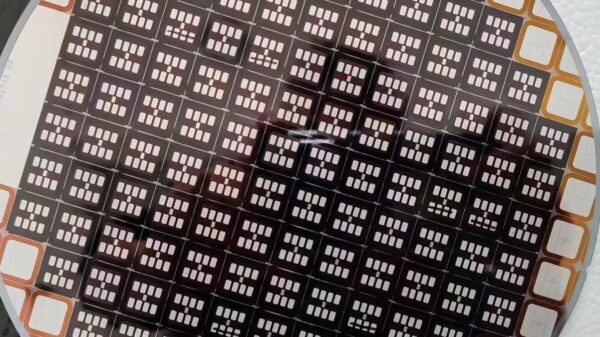
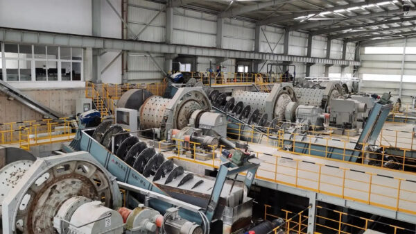


In a bold move that has triggered protest from Beijing, the Japanese government has unveiled a rigorous export control strategy to curtail China’s burgeoning semiconductor sector. The new regulations will impose stringent controls on the export of key semiconductor manufacturing equipment, including extreme ultraviolet (EUV) lithography and advanced etching equipment.
Japan’s Ministry of Economy, Trade and Industry (METI) announced on May 23 that it would be expanding its export control regulations to include 23 new items essential for high-tech semiconductor manufacturing. This move mandates Japanese firms to obtain explicit permission from the government before exporting these items to a list of countries outside an established group of 42 ‘friendly’ nations. The tightened export controls are set to take effect on July 23.
Although METI has not specifically designated a target nation, international media, including Nihon Keizai Shimbun, are interpreting the restrictions as primarily aimed at China. This is seen as a response to US calls for greater regulation on semiconductor exports.
China’s Ministry of Commerce has promptly denounced Japan’s new export restrictions, citing them as a violation of free trade and international economic regulations. “This is an egregious abuse of export control measures,” the ministry said in a statement. “China firmly opposes this.”
Japan’s new regulatory constraints are likely to impede China’s ongoing efforts to bolster its domestic semiconductor industry. Despite substantial investments, China’s semiconductor sector has faced challenges in manufacturing advanced equipment, creating an opportunity for Japanese giants such as Tokyo Electron, Advantest, Nikon, and Canon.
Following the announcement of the new regulations, shares in Chinese semiconductor manufacturers, including SMIC and Hwahong Semiconductor, fell by 6.5% and 4.6% respectively.
Amidst this escalating trade dispute with China, Japan appears to be courting the South Korean semiconductor industry. On May 22, Japan’s Minister of Economy, Trade and Industry, Yasutoshi Nishimura, extended a warm welcome to Samsung Electronics’ proposed plans to establish a new base in Japan, promising full support.
Samsung Electronics is reported to be planning an investment of JPY 30 billion (around $216 million) to set up a semiconductor post-process R&D base in Yokohama, Japan. The Japanese government is believed to be offering subsidies worth more than JPY 10 billion ($71.9 million) to facilitate this move.
In a broader approach, METI has also signaled its readiness to extend subsidy support to other South Korean semiconductor firms. Minister Nishimura said, “While no concrete proposals have yet been received, we will evaluate potential partnership opportunities that could further strengthen our relationship with South Korea.”