


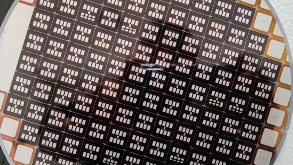


The demand for high-performance semiconductors has led to rapid advancements in process miniaturization and the proliferation of 2.5D and 3D packaging. Consequently, the complexity of semiconductor design has increased dramatically. To address this complexity, the industry is actively seeking ways to leverage AI technologies in electronic design automation (EDA) tools, aiming to reduce both development costs and time.
During the recent ‘2023 Advanced Semiconductor Package Innovation Process Conference’ in Seoul, Han Man-yong, managing director of Cadence Korea, highlighted that machine learning-based AI design tools are quickly being commercialized within the semiconductor design arena. This development has the potential to significantly accelerate the semiconductor development process for many companies.
Cadence is a global frontrunner in EDA tools, catering to major clients like Samsung Electronics, SK Hynix, and TSMC. The complexity of semiconductor design is expected to continually increase due to the emergence of cutting-edge technologies, such as process miniaturization and 2.5D and 3D packaging.
In the near future, I anticipate large-scale deployment of AI machine learning-based functions, such as the TSV optimizer, which supports customers in semiconductor design. Although many AI features are yet to be introduced, companies like Cadence are actively expanding the implementation of AI technology in their solutions.
The integration of AI capabilities into EDA tools is not an exclusive pursuit of Cadence. Notable competitors, including Synopsys and Siemens EDA, are also extending the application of AI technology to their EDA tools. For instance, Synopsys has introduced the DSO.ai tool, which employs AI technology to optimize layout arrangements in the semiconductor design stage. This tool allows for more efficient layout arrangement optimization compared to human engineers.
Advanced packaging design is another area of interest. The Integrity 3D-IC Platform was showcased at the event, enabling simulations such as testing optimal 3D structure layout scenarios during the design process. This platform reduces development costs and time in the advanced packaging stage.
In my opinion, the 3D-IC package field, despite being in its infancy, has attracted the interest of leading domestic and international companies. I foresee rapid growth in the 3D-IC package field as the industry continues to innovate and explore advanced packaging solutions.